Scanning Tunneling Spectroscopy of Insulating Films
Paper for Advanced Solid State Physics class, Dmitri Y. Petrovykh.
Physics Department, University of Wisconsin, Madison, WI, USA (1999)
-
1 STM and STS of Bulk Insulators
2 STS of Thin Film Insulators -
1 Tunneling Current Theory
2 Tunneling Barrier Parameters
3 The Simplest Model for T(E,V)
4 Thermal Broadening Included
5 More Accurate Tunneling Probabilities - Possible Additional Effects
- Acknowledgments & References
II.3 The Simplest Model - T(E,V) Dependence Only
In the simplest approximation one can neglect the effect of a finite temperature and consider sharp step functions instead of the Fermi function f(E) for metallic density of states. The tunneling probability through the insulator Tins is assumed to be:
Tins(E,V) = exp[ 2a (ECBMeVE)½ dins] for eV+E < ECBM
Tins(E,V) = 1 for eV+ E > ECBM
Electrons tunneling into the gap see a constant height barrier, and electrons tunneling into the conduction band of the insulator propagate freely.

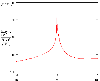
Fig. 3 Normalized conductance calculated including the
contribution from the tunneling probability only.
Adjustable parameters:
dins = 3 Å
ECBM = 3 eV
Amazingly enough, even this simplest model produces the resonant peak at CBM in normalized conductance (Fig. 3), and the absolute values that are not too far from the observed ones (compare to Fig. 2). Typical values are assumed for the insulator thickness dins and ECBM.
