Chemical Imaging with STM
CaF2 (Calcium Fluoride) on stepped silicon is an interesting system to study, because it opens the possibility of creating various nanostructures. The small size of these structures makes STM the primary analytical tool. The caveat, however, is that CaF2 is an insulator, and thus it is surprising that any STM imaging is possible at all for this system.

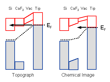
Fig. 1 Schematic of chemically-selective
tunneling into insulator films, using CaF2 on Si(111)
as example.
Left: Stabilizing the
tip at a sample bias that allows tunneling of electrons from the
tip into the conduction band minimum (CBM) of the insulator.
Right: Acquiring a current
image at a bias where electrons from the tip enter the gap of
the insulator.
Bands with empty states are outlined with red, filled
states—blue and shaded gray. Dashed line marks EF.
Scanning Tunneling Microscopy (STM) imaging seems to be hardly possible for insulating surfaces, since the tunneling current will be very efficiently attenuated inside the insulating film. The only way to avoid this exponential dampening of the tunneling current is to inject electrons into the conduction band of the insulator, where they should be able to propagate. A typical insulator has an optical forbidden energy gap of about 10 eV and such extreme bias voltages are not practical for STM.
Fortunately, for an insulator film grown on a semiconductor substrate, the energy difference between the conduction band minimum (CBM) and the Fermi energy (EF) can be smaller than the gap because of the band alignment. Fig. 1 (left) illustrates this phenomenon for the case of CaF2 film on Si(111) substrate. The Fermi level of the system is pinned near the top of the Si valence band. The top of the valence band of bulk-like CaF2 is placed at 8.5 eV below EF. Therefore, even though the band gap of CaF2 is 12 eV, the CBM should be only about 3.5 eV above EF. So STM imaging is in fact possible for positive sample biases of 3.5 eV and above4,5. Attempts to stabilize the tunneling current at a bias voltage below the CBM causes the tip to approach the underlying Si and to pick up insulating CaF2 debris or crash-land on the sample.

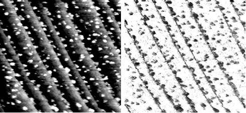
The method described above indeed works as can be seen from the presented images. The one on the left is a 100×80 nm2 topography image taken with 3.8 V bias (CaF2 appears bright, Si—dark), the right image taken with +2 V bias exhibits the reverse chemical contrast (i.e. CaF2 appears dark, Si—bright).
