Scanning Tunneling Spectroscopy of Insulating Films
Paper for Advanced Solid State Physics class, Dmitri Y. Petrovykh.
Physics Department, University of Wisconsin, Madison, WI, USA (1999)
Scanning Tunneling Spectroscopy (STS) measurements for insulating systems are notoriously difficult and often yield ambiguous results because of exponentially vanishing tunneling currents for biases within the forbidden energy gap of insulators. This inherent limitation can be circumvented by measurements in films only few atomic layers thick. In recent experiments with CaF2 films on Si(111) an unexpected peak in STS spectra has been found at energy close to that of conduction band minimum of CaF2. This result is interpreted using simple models of tunneling through thin insulating films.
-
1 STM and STS of Bulk Insulators
2 STS of Thin Film Insulators -
1 Tunneling Current Theory
2 Tunneling Barrier Parameters
3 The Simplest Model for T(E,V)
4 Thermal Broadening Included
5 More Accurate Tunneling Probabilities - Possible Additional Effects
- Acknowledgments & References
I.1 STM and STS of Bulk Insulators
Scanning Tunneling Spectroscopy (STS) over the last decade has proven to be a very valuable tool in studies of clean metal and semiconductor surfaces and various adsorbates on these surfaces1,2. Application of this technique to insulators however faces two major obstacles.
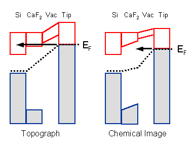
Even Scanning Tunneling Microscopy (STM) imaging seems to be hardly possible for insulating surfaces, since the tunneling current will be very efficiently attenuated inside the insulating film. The only way to avoid this exponential dampening of the tunneling current is to inject electrons into the conduction band of the insulator, where they should be able to propagate. A typical insulator has an optical forbidden energy gap of about 10 eV and such extreme bias voltages are not practical for STM. Fortunately, for an insulator film grown on a semiconductor substrate, the energy difference between the conduction band minimum (CBM) and the Fermi energy (EF) can be smaller than the gap because of the band alignment. Fig. 1 (left) illustrates this phenomenon for the case of CaF2 film on Si(111) substrate. The Fermi level of the system is pinned near the top of the Si valence band. The top of the valence band of bulk-like CaF2 is placed at 8.5 eV below EF. Therefore, even though the band gap of CaF2 is 12 eV, the CBM should be only about 3.5 eV above EF. So STM imaging is in fact possible for positive sample biases of 3.5 eV and above4,5. Attempts to stabilize the tunneling current at a bias voltage below the CBM causes the tip to approach the underlying Si and to pick up insulating CaF2 debris or crash-land on the sample.

Fig. 1 Schematic of chemically-selective
tunneling into insulator films, using CaF2 on Si(111)
as example:
Left: Stabilizing the
tip at a sample bias that allows tunneling of electrons from the
tip into the conduction band minimum (CBM) of the insulator.
Right: Acquiring a current
image at a bias where electrons from the tip enter the gap of
the insulator.
Bands with empty states are outlined with red, filled
states - blue and shaded gray. Dashed line marks EF.
In STS mode, the feedback loop of the STM is turned off, the bias voltage is ramped between the specified values and the tunneling current is recorded. Thus an I(V) curve is obtained in one point above the surface. The procedure can be repeated for multiple points (usually a square array). Note, that during the motion between these points the feedback loop has to be on, which means that a specified sample bias - tunneling current combination is maintained. Again, for insulators the bias needs to be rather high (e.g., 3.5 eV for CaF2, as explained above), which effectively limits the bias range available for STS2. Basically the tunneling current drops exponentially for bias voltages smaller than the stabilization value, and since a typical setup only has sensitivity that spans a few decades, the smallest possible bias voltage is limited by the smallest detectable tunneling current. That problem can be somewhat alleviated either by the correct choice of stabilization parameters, or by employing other STS techniques2.
The second obstacle of performing STS with insulators is related to the interpretation of the STS data. The I(V) curve is dominated by the exponential dependence of the tunneling current I on the bias voltage V. One way to obtain sample specific information is to calculate (dI/dV)/(I/V)—a quantity called normalized conductance, which has been shown to approximate the density of states of the sample2,6. The problem is that for bias voltages below the CBM the tunneling current I = 0 for bulk insulators and semiconductors, while the conductance (dI/dV) remains finite. The normalized conductance (dI/dV)/(I/V) thus has a singularity near the CBM, which has been experimentally observed for bulk semiconductors7. The appearance of this singularity can be avoided by using alternative forms of the normalized conductance, but one has to be careful not to introduce any artifacts into the resulting spectra.
