Scanning Tunneling Spectroscopy of Insulating Films
Paper for Advanced Solid State Physics class, Dmitri Y. Petrovykh.
Physics Department, University of Wisconsin, Madison, WI, USA (1999)
-
1 STM and STS of Bulk Insulators
2 STS of Thin Film Insulators -
1 Tunneling Current Theory
2 Tunneling Barrier Parameters
3 The Simplest Model for T(E,V)
4 Thermal Broadening Included
5 More Accurate Tunneling Probabilities - Possible Additional Effects
- Acknowledgments & References
I.2 STS of Thin Film Insulators
The normalization problem described in the previous section can be averted if we utilize thin films, where the tunneling current I remains finite inside the band gap. The states of the silicon substrate decay exponentially through the CaF2 film, leaving a finite density of states at the CaF2 surface available for tunneling.

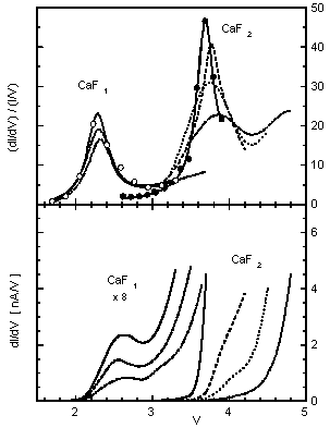
Fig. 2 Tunneling spectra of CaF1/Si(111)
and CaF2/CaF1/Si(111).
Two sharp onsets in the (dI/dV) spectra characterize the respective
conduction band minima and provide chemical selectivity. The normalized
(dI/dV)/(I/V) spectra exhibit resonances at the CBM. Different
line types represent different tip-sample separations.
The experimental5 (dI/dV)/(I/V) tunneling spectra obtained from CaF2/Si(111) and CaF1/Si(111) interfaces are presented in Fig. 2. The conduction band edges correspond to onsets in the (dI/dV) curves. In the normalized spectra well-defined peaks are observed at the CBM. The peak is three times as high as the continuum above it for CaF2 and five times as high for CaF1. In search of an explanation for this phenomenon several options can be considered5. Here a model for tunneling through a thin insulator film is developed, based on established approaches for planar tunneling6. The outcome produces the observed resonances and even their absolute height, suggesting that the most important physical effects are indeed captured in the model with a simple barrier structure. Some possible extensions of this approach for more realistic barrier potentials will be discussed as well.
