Scanning Tunneling Spectroscopy of Insulating Films
Paper for Advanced Solid State Physics class, Dmitri Y. Petrovykh.
Physics Department, University of Wisconsin, Madison, WI, USA (1999)
-
1 STM and STS of Bulk Insulators
2 STS of Thin Film Insulators -
1 Tunneling Current Theory
2 Tunneling Barrier Parameters
3 The Simplest Model for T(E,V)
4 Thermal Broadening Included
5 More Accurate Tunneling Probabilities - Possible Additional Effects
- Acknowledgments & References
II.2 Tunneling Barrier Parameters
The first approximation is to assume that both the tip and the sample are essentially metallic and have the same work function φ and constant density of states. The assumption of a constant tip density of states is often made, lacking detailed knowledge of the tip states. The Si density of states has little structure at the energies under consideration, i.e., about 4 eV above the valence band maximum.
Assume that the tunneling probability through the vacuum is given by:
Tvac(E,V) = 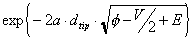 ,
where
,
where 
which corresponds to WKB approximation for tunneling through a barrier of the average height.
Assume that the total tunneling probability T(E,V) = Tvac(E,V)Tins(E,V).
The following are the values of the "fixed" tunneling barrier and environment parameters:
- φ = 4 eV — work function for the tip and the sample,
- kT = 0.026 eV — assume room temperature,
- dtip = 11 Å — tip-sample separation (typical value for sample bias of 3–4 V),
- dins — thickness of the insulator film in Å.
These are the values used in all the following models, unless specified otherwise.
Main page: Chemical contrast STM | Next section: The Simplest Model for T(E,V) »
 surface")