Scanning Tunneling Spectroscopy of Insulating Films
Paper for Advanced Solid State Physics class, Dmitri Y. Petrovykh.
Physics Department, University of Wisconsin, Madison, WI, USA (1999)
-
1 STM and STS of Bulk Insulators
2 STS of Thin Film Insulators -
1 Tunneling Current Theory
2 Tunneling Barrier Parameters
3 The Simplest Model for T(E,V)
4 Thermal Broadening Included
5 More Accurate Tunneling Probabilities - Possible Additional Effects
- Acknowledgments & References
II.1 Tunneling Current Theory
Since the appearance of the STM most tunneling theories are based on Bardeen's tunneling current formalism8, which has been adapted for the STM by Tersoff and Hamann9:

where f(E) is the Fermi function, V - the bias voltage, Mμν—the tunneling matrix element between the states ψμ of the tip and ψν of the surface. In special cases Mμν and the whole above expression can be simplified. In a particular case of interest to STS of semiconductors and insulators, we are dealing with the applied bias of the order of 2 eV, which is not small in comparison to kT (0.026 eV at room temperature). For tip-sample bias smaller than a typical work function (4–5 eV) the tunneling current at a fixed location on the surface can be approximated6 as:
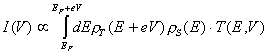
where ρT(E+eV) is the density of states of the tip, ρS(E) is the density of states of the sample and T(E,V) is the transmission probability of the electron of energy E through the tunneling barrier. Even in this simplified model, a number of assumptions about all the three functions in the integrand can be made to construct more or less realistic models. Several such models will be considered in the following sections.
Main page: Chemical contrast STM | Next section: Tunneling Barrier Parameters »
 surface")