Scanning Tunneling Spectroscopy of Insulating Films
Paper for Advanced Solid State Physics class, Dmitri Y. Petrovykh.
Physics Department, University of Wisconsin, Madison, WI, USA (1999)
-
1 STM and STS of Bulk Insulators
2 STS of Thin Film Insulators -
1 Tunneling Current Theory
2 Tunneling Barrier Parameters
3 The Simplest Model for T(E,V)
4 Thermal Broadening Included
5 More Accurate Tunneling Probabilities - Possible Additional Effects
- Acknowledgments & References
II.4 Thermal Broadening Included via f(E)
The next logical step is to include the effects of the thermal broadening that will be present to some extent at room temperature. It is done by assuming Fermi distribution for the occupied states in both the tip and the sample. That is assume:
ρS (E) ~ 1 - f(E)
ρT (E) ~ f(E)
f(E) = 1 / (exp[E/kT]+1)
It appears that at this stage the model captures the essence of the process, so it will be examined in some detail. First we should assign realistic values to dtip and dins. In case of CaF2 (Fig. 2 right curves) the stabilization bias voltage was about 4 V, which corresponds to about 11 Å tip-sample separation. CaF2 layer grows on top of CaF1, so if we take CaF2 layer + the fluorine plane from CaF1 layer as the insulator, the thickness should be 1¼*3.14 = 3.93 Å. Similarly, for CaF1 (Fig. 2 left curves) the tip was stabilized at about 3.5 V (dtip = 10 Å) and the insulator layer thickness is 2.7 Å. Now, the only adjustable parameter in the model is the position of the CBM. Since in this model the peak position coincides with ECBM, we can set it to 2.3 eV for CaF1 and 3.7 eV for CaF2, to match the observed values from Fig. 2. The dI/dV and (dI/dV)/(I/V) curves obtained from this model are presented in Fig. 4. Note the similarity to Fig. 2, even in the absolute values of the normalized conductance. Such similarity is surprising for modeling results with basically no adjustable parameters.

Fig. 4 Calculated tunneling spectra obtained from a minimal model for tunneling through an insulator film. Spectra are shown for CaF2 and CaF1, analogous to the data in Fig. 2.
The model also provides some predictions, such as the dependence of the peak height on ECBM and dins. The resonance peak basically scales with both in bilinear fashion:
(dI/dV)/(I/V)max ~ 2.4 (eV Å)-1 dins ECBM (see overview in Fig. 5)
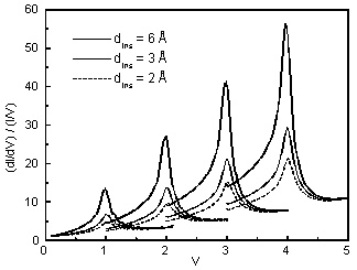
Fig. 5 Peak height dependence on ECBM and dins.
Another very important observation, is that as dins tends towards infinity, so does the peak height. As it was pointed out before, in practice there is always the smallest detectable tunneling current limiting our observations for thick (i.e., bulk-like) films, so only a certain range of the normalized conductance will be observed. If the peak height corresponding to a particular film thickness is sufficiently greater than the observable range, than the normalized conductance will appear to have a singularity as it approaches ECBM (Fig. 6). For ECBM = 4 eV asymptotic dins approaches infinity behavior is reached already for film thickness 15 Monolayers (ML). But finite peaks in the normalized conductance should still be observed for 1-5 ML thick insulator films, with this limiting width decreasing with increasing ECBM.
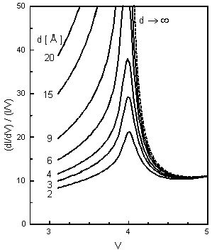
Fig. 6 Apparent singularity in (dI/dV)/(I/V) near ECBM = 4 eV, as insulator thickness d tends towards infinity.
It is interesting to note that this modeling of the singular behavior seems to be quite universal. In Fig. 7 the model's prediction is compared to the actual data for bulk GaAs. Note that in this case the only adjustable parameter in the model was the value of ECBM = 1.02 eV, which was assigned in the original paper by Martensson and Feenstra7.
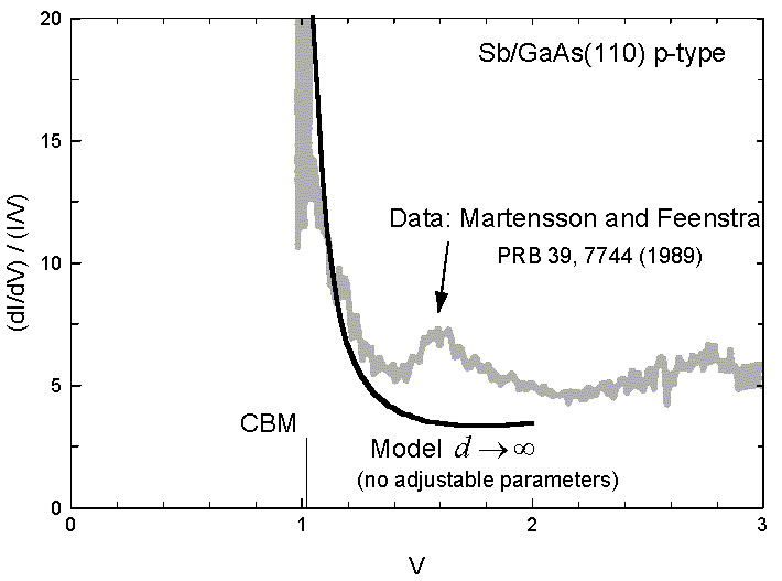
Fig. 7 Normalized conductance singularity near ECBM. Comparison of the model curve with data for bulk GaAs.
Main page: Chemical contrast STM | Next section: More Accurate Tunneling Probabilities »
 surface")