Stepped Silicon Surfaces
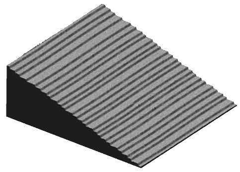
One very powerful way to create atomic- or nano-scale structures in a controlled manner is to use stepped silicon surfaces as templates. To obtain such stepped surfaces, Silicon crystals are cut at a small angle with respect to a highly stable crystal plane [in this case Si(111) plane]. The surface then attempts to maintain the preferred orientation, but is forced by the miscut to form atomic steps every so often. These steps are separated by atomically flat terraces and the width of these terraces is determined by the miscut angle. Below is a 3-dimensional representation of an STM image of a Si(111) stepped surface.

The area shown is about 400×400 nm2, flat terraces are on average 15–17 nm wide. Each one of the steps on this atomic staircase is approximately 0.3 nm high, so the vertical axis is stretched by a factor of 15 to show the steps.

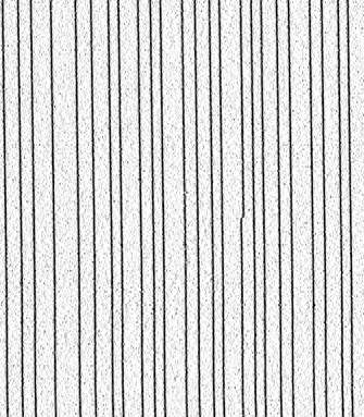
Note how straight the steps are - this can be seen better on the image on the left, which is basically the top view of the surface shown above. Or rather, it is the top view with illumination from the left (STM image in the derivative mode). Downhill is to the right and steps appear as dark lines.
There is only one kink (close to the center of the image) in the whole area, the rest of the steps are, in fact, atomically straight. It turns out that the 7×7 reconstruction of this surface is responsible for the straightness of the steps.
These perfect nanoscale templates can be used to create uniform atomic chains and other low-dimensional structures.
