Si(111) Surface
Diamond Lattice

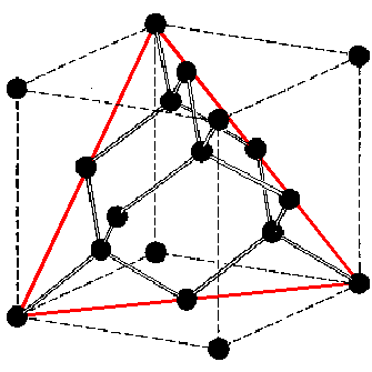
Silicon has a crystal lattice of the diamond lattice structure (see the schematic view on the left).
Si(111) notation refers to a specific set of atomic planes in that structure. In the cube shown on the left it corresponds to the plane outlined with red.
Another way to see what the (111) crystal planes in diamond lattice look like is provided by the "cork-ball" models shown below.
Si(111) Surface
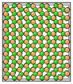
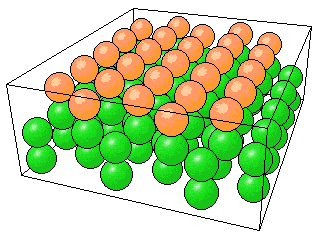
The left image shows a top view of the atomic arrangement for the (111) plane. The right image shows a 3-dimensional view of the same surface. In both cases atoms are color-coded: orange for the top layer, green for all the deeper layers.


These two images have been generated with the help of the Surface Explorer web-based tool.
7×7 Reconstruction of Si(111)
When a (111) surface of Silicon is heated to sufficiently high temperature under the ultra-high vacuum (UHV) conditions, the surface atoms rearrange into a more energetically stable configuration called the 7×7 reconstruction. Instead of a very simple pattern shown above, the new arrangement involves several types of atomic positions in the top three atomic layers to form a much larger unit cell.
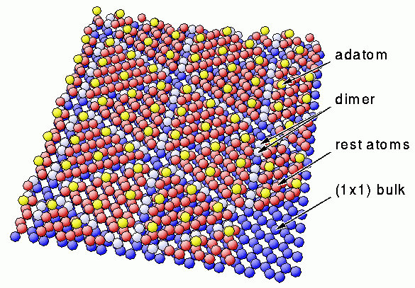
A model of this new 7×7 surface structure is shown below. Color-coding indicates different types of Silicon atoms from the top three atomic layers that are involved in forming the 7×7 reconstruction. The "Dimer-Adatom-Stacking fault" (DAS) model (Takayanagi/Tong) indicates that the most prominent features observed in STM images correspond to adatoms (shown in yellow). This model also clearly shows corner-holes, i.e., areas at the corners of the 7×7 unit cells where atoms from the top three layers are missing. Corner-holes appear in STM images as dark areas surrounded by hexagons of adatoms or, on a larger scale, by six triangles, each triangle, in turn, composed of six adatoms.

Image from the gallery based on the Surface Structure Database (SSD, NIST Standard Reference Database 42) by P. R. Watson, M. A. Van Hove, K. Hermann. The image has been prepared from SSD output and postprocessed with BALSAC by K. Hermann.
Below is a 3D representation of an STM image of Si(111)7×7 with several unit cells shown. The corner-holes correspond to the corners of the unit cell, the atoms imaged as bright protrusions are adatoms. For a semiconductor, such as Silicon, an STM image is quite close to the actual atomic arrangement on the surface.
The area of this image is 18×8 nm2, and the height of the "bumps" is only about 0.04 nm—a fraction of atomic size.
