Single-domain Ca-Si(111)3×1 Reconstruction
3×1 or 3×2 Structure?
Basic considerations suggest that Ca-Si(111)3×1 reconstruction is an anisotropic surface structure that could exhibit one-dimensional (1D) behavior. The quotation marks around "3×1" assignment, however, indicate a controversy regarding the actual atomic arrangement. Almost all studies with diffraction techniques (LEED, RHEED) produce a typical 3×1 pattern. STM observations, on the other hand, indicate a 3×2 arrangement, which agrees with photoemission results. In fact, a structural model of a 3×2 reconstruction in a similar Ba-induced system suggests the most elegant way to reconsile the various experimental observations.
STM Image of Atomic Chains
An STM image of the rows of the Ca-Si(111)3×1 reconstruction shows a "zig-zag" pattern typical for other 3×1 reconstructions on Si(111), most of which are induced by alkali metals.
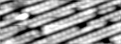
9×3 nm2 filled-states STM image, experiment in collaboration with F. M. Leibsle (UMKC).
Structural Models of Zig-zag Chains
Two types of structures are proposed for these zig-zag chains.
First model (left image below) associates the observed bright protrusions with actual
atoms (or atomic orbitals) arranged in a zig-zag manner.
Second type of models
(right image below) assumes a chain of ring-like structures instead, and associates the bright spots with
two edges of the rings.
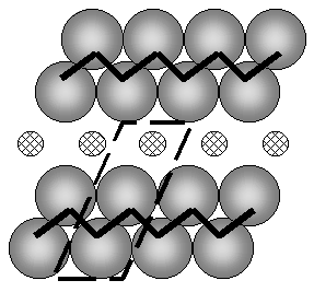
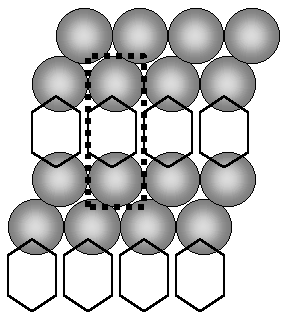
Grey circles in the above images represent the protrusions seen in STM images, unit cells for the 3×1 structures are outlined with thick dashed lines.
Chains of Atoms or Rings?
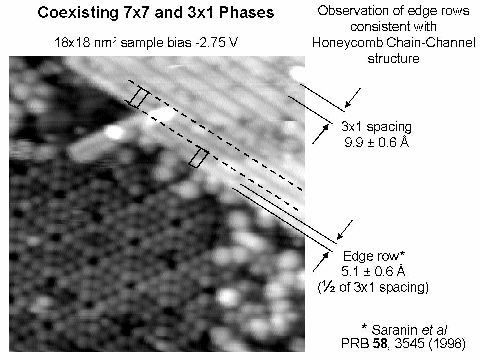
Even basic considerations, e.g., those of typical bond lengths, are not very consistent with a simple zig-zag chain of atoms. In contrast, the ring-like model tends to explain the observed STM images well. Another strong supporting evidence for the ring-like structural element is the observation of the edge row features. Basically, rows on the boundaries of the 3×1 domains are of bright-dark-bright structure consistent with the ring-like structural units, but inconsistent with a double-wide-bright-dark structure expected for a chain-like arrangement.
Single-domain 3×1 Reconstruction
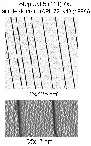
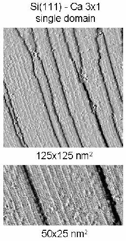
Before one sets out to do an angle-resolved PES measurement, uniformity of the sample structure across a macroscopic scale needs to be ensured. Looking for 1D signatures is also much easier if the reconstruction is single-domain, i.e., all the rows are along the same direction. As seen below, using vicinal silicon substrates produces the desired high-quality single-domain Ca-Si(111)3×1 samples.
Photoelectron Spectroscopy
Of course the prize in the hunt for 1D surface structures is to find a metallic surface state that has 1D character. Alkali-induced 3×1 reconstructions have been always found to be semiconducting. If the structure of a 3×1 unit cell remains the same, then from the simple principles of electron counting, the exchange of a monovalent alkali atom by a divalent Ca should change the count from even to odd and the system from semiconducting to metallic.
Unfortunately, excellent samples notwithstanding, no 1D or even just a metallic state is observed for this system, as shown in the photoemission data below. The absence of a metallic state was a real mystery initially, because the electron count principles can not be violated.
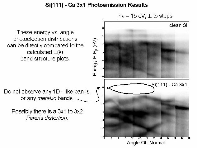
Of course, the electron count is not violated in Ca-Si(111)3×1. Rather, the structure of a "3×1" unit cell is changed. In fact, a metal atom is only present in every one of the 3×1 cells, making a 3×2 structure and producing an even electron count. More details can be found in Petrovykh et al., Surface Science 512, 269 (2002) and in other publications.
