Single-domain Au-Si(111)5×2 Reconstruction
5×1 or 5×2 Structure?
Deposition of 0.2–0.4 ML of gold on Si(111) at about 600°C results in a uniform single-domain surface reconstruction. From the LEED pattern it appears to be 5×1, whereas STM clearly shows 5×2 structure, hence the structure is often denoted as "5×1". When STM tip picks up a gold atom into a stable configuration, stable atomic resolution STM imaging becomes possible on this surface.
Atomic-Resolution STM Images

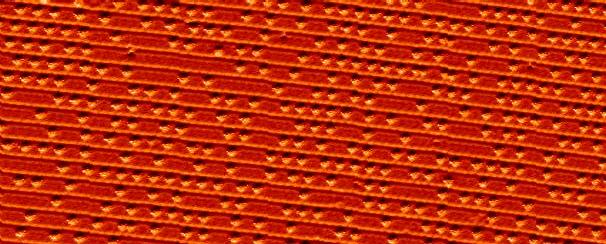
75×25 nm2 STM image of atomic rows on Au-Si(111)5×2 (derivative mode).
There are three types of features in the above STM image.
- Rows of 5×2 reconstruction.
- Prominent protrusions on top of the rows.
These protrusions are associated with extra gold atoms, the corresponding smallest spacing is ×4 along the rows. - A string of small protrusionst at the edge of each row.
The spacing of these small protrusions corresponds to the 5×2 periodicity.
Atomic Chains
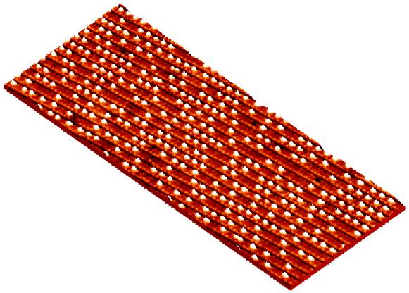
The following image shows a three-dimensional representation of atomic chains on Au-Si(111)5×2.

Photoelectron Spectroscopy
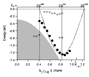
Does the Au-Si(111)5×2 surface have a one-dimensional metallic band?
Photoemission results show a strong band with dispersion along the reconstruction rows and with minimal dispersion in the perpendicular direction. But that band does not cross the surface Fermi level, so it likely undergoes Peierls distortion.

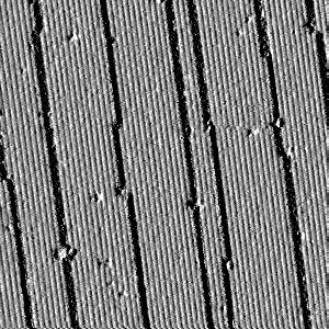
100×100 nm2 STM image of Au-Si(111)5×2 rows.

1D dispersion of the Au-Si(111)5×2 surface band.
Additional Information
Prof. Himpsel's page at the University of Wisconsin provides more information about these atomic wires.
