Spin-Polarized Scanning Tunneling Microscopy
Literature Review by Dmitri Y. Petrovykh
- Introduction
- SPSTM Basics
- Spin-Polarized Tunneling
- SPSTM with Magnetic Tips
- Optically Pumped Tips
- SPSTM Q&A
- References
V. Optically Pumped GaAs Tips
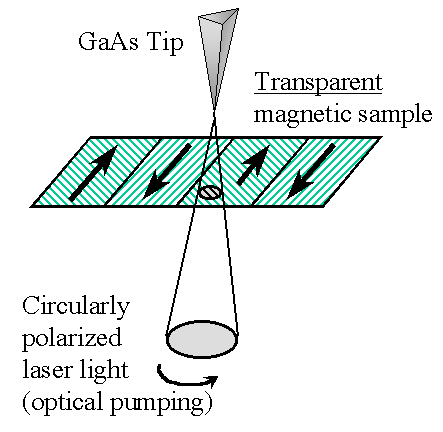
As promising as magnetic tip SPSTM is, it is not the only existing approach to obtain spin-polarized tunneling. Probably the most refined alternative is the use of optically pumped GaAs tips as sources of spin-polarized electrons. This technique can be used to study semitransparent (i.e., thin film) magnetic samples. An example of a possible experimental setup is summarized in Fig. 4. A GaAs tip is mounted on a regular STM and scanned across a sample. At the same time a beam of circularly polarized laser light is focused on the apex of the tip. To obtain the best possible polarization the laser light has to come perpendicular to the sample, that is why a semitransparent sample is used and laser beam is illuminating the tip through the sample.

Fig. 4 Setup for SPSTM with optically pumped GaAs tip.
It has been shown22 that due to spin-orbit coupling and optical selection rules in GaAs, spin-polarized electrons can be induced by circularly polarized light. A bias voltage is applied between the tip and the sample, creating small tunneling current of these spin-polarized electrons. As it was illustrated in section III, the spin-polarized tunneling current depends on the direction of the sample's magnetization and therefore can be used to image the magnetic structure of the sample.
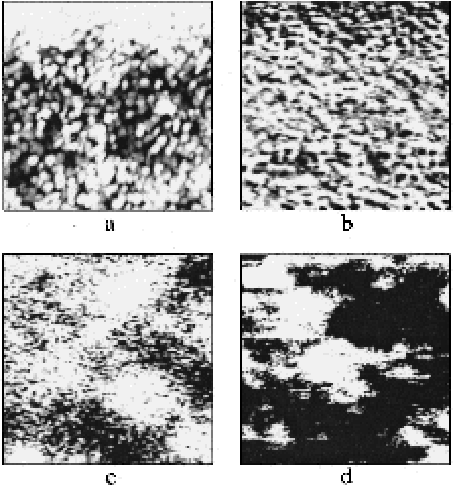
The practical implementation of the deceivingly simple scheme from Fig. 4 was thoroughly investigated in a series of papers22,23 by Prince et al. and recently observation of magnetic domains of Co films (see Fig. 5) was observed by Suzuki et al.24 using an STM with optically pumped GaAs tips.

Fig.5 (a) Topography image; (b) intensity modulation image; (c) polarization modulation response image. These 1×1 μm2 images were recorded at the same sample location. (a) & (c) are simultaneous. (d) 1×1 μm2 MFM image obtained on a typical sample with 10 nm gold-covered layer. (Adapted from Ref. 24)
Topography image (Fig. 5a) shows the grainy structure of the sample (thin Co film on a 10 nm gold/mica substrate) due to the gold grains. The variation in laser beam intensity (Fig. 5b) does not affect that small-scale graininess of the image, but does not induce any larger-scale (few 100 nm) structure. However polarization image (Fig. 5c) does exhibit large-scale contrast that is very similar to a typical Magnetic Force Microscopy (MFM) image (Fig. 5d) of the same type of sample. This result certainly does suggest that in fact the magnetic contrast was obtained, and leaves the possibility of nm and sub-nm resolution open. While obviously free of any problems due to magnetostatic tip-sample interactions (the tip is not magnetic!), this approach does have caveats of being limited to studies of thin films and of poor general understanding on the effects of the laser illumination on the nm scale, such as energy dependence and possible heating.
