Spin-Polarized Scanning Tunneling Microscopy
Literature Review by Dmitri Y. Petrovykh
- Introduction
- SPSTM Basics
- Spin-Polarized Tunneling
- SPSTM with Magnetic Tips
- Optically Pumped Tips
- SPSTM Q&A
- References
IV. SPSTM with Magnetic Tip and Magnetic Sample
Even though their detailed observations and predictions vary significantly, spin-polarized tunneling experiments provide us with all the necessary tools for SPSTM. The idea is to use a single crystal ferromagnet with constant magnetization as an STM tip, while imaging a sample that in the simplest case should be also a single crystal ferromagnet.
If the tip has a properly chosen well-defined crystal plane at its end, when bias voltage is applied the tip becomes a source of spin-polarized electrons and a ferromagnet-insulator-ferromagnet junction is formed between the tip and the sample. The tunneling current then should depend on the orientation of the sample's magnetization with respect to the spin-polarization of tunneling electrons (Fig. 2). Direction of the local magnetization changes from domain to domain, thus magnetic structure can be imaged with nm and sub-nm resolution typical for STM.
Substantially polarized tunneling electrons are necessary to produce easily detectable variation (on the order of 10 %) of the tunneling current caused by the orientation of the sample magnetization. There are at least 4 ferromagnetic metals that can be sources of such polarized electrons (see Table 1).
Table 1
Spin polarization of electrons tunneling
from ferromagnetic materials10
| Metal | Spin polarization (%) |
| Fe | + 40 +/- 2 |
| Co | + 35 +/- 3 |
| Ni | + 23 +/- 3 |
| Gd | + 14 +/- 3 |
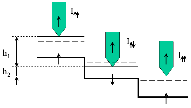
A prototype SPSTM with single-crystal Ni tip was in fact built, tested and reproducible signals consistent with spin-polarized tunneling were reported16. However the first SPSTM results in vacuum were actually obtained by Wiesendanger et al.17 using a different magnetic tip—CrO2-covered cleaved Si(111). In that experiment a Cr(001) surface with atomic steps was imaged using non-magnetic (W) and then magnetic tip. Height of all the steps appeared to be the same (0.14 nm) while imaging with non-magnetic tip, but showed alternation between 0.16 and 0.12 nm with magnetic tip. Authors point out that this can be easily explained by the model where steps on Cr sample have alternating magnetization (see Fig. 3).

Fig. 3 Ferromagnetic tip scanning over alternately magnetized terraces separated by monoatomic steps. A contribution from spin-polarized tunneling leads to larger apparent height h1 for parallel tunneling, compared to smaller h2 for antiparallel tunneling. (Adapted from Ref. 17)
Although still open for alternative explanations, taken at face value this observation suggests that use of SPSTM for imaging of magnetic structures is indeed possible. In this light, it is very encouraging that atomic resolution in magnetic tip - magnetic sample system has been reported21 by the same group 2 years after the first experiments. This sub-nm resolution has been achieved with an iron tip on (100) surface of magnetite (Fe3O4) where images show individual rows of iron ions (0.59 nm row spacing). More recently successful Scanning Tunneling Spectroscopy (STS) of Fe/W(110) system using iron covered tungsten tips was reported18 by the same group, opening the possibility for magnetically sensitive spectroscopy measurements.
Use of other tip materials can be advantageous for several practical reasons. First, significant increase in polarization of emitted electrons has been observed when metallic electrodes were covered with thin film of EuS. After the fisrt experiments19 in the 70's this "spin-filter" effect has been observed for few other similar materials and is generally attributed20 to the effect of tunneling barrier caused by exchange splitting. Such splitting lowers the tunnel barrier energy for spin-up and raises it for spin-down electrons, leading to the preferential selection of spin-up electrons in the tunneling current.
Magnetostatic interaction between a ferromagnetic tip and a ferromagnetic sample is another example of a practical problem that can be solved by using an alternative material - in this case antiferromagnetic tip! A wide range of conducting antiferromagnetic compounds was studied21 for that purpose and Cr, MnNi and MnPt tips produced atomic resolution imaging on non-magnetic samples during testing21.
